![]()
![]()
![]()
![]()

| FEATURES | TYPICAL APPLICATIONS | |||||||||||||||||||||||||||||||||||||||||
| 1). Center amplifying gate | ). DC motor controls | |||||||||||||||||||||||||||||||||||||||||
| 2). Hermetic metal case with ceramic insulator | 2). Controlled DC power supplies | |||||||||||||||||||||||||||||||||||||||||
| 3). International standard case TO-209AE (TO-118) | 3). AC controllers | |||||||||||||||||||||||||||||||||||||||||
| 4). Threaded studs UNF 3/4 - 16UNF2A or ISO M24x1.5 | ||||||||||||||||||||||||||||||||||||||||||
| 5). Compression Bonded Encapsulation for heavy duty | 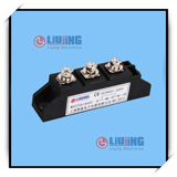 | |||||||||||||||||||||||||||||||||||||||||
| operations such as severe thermal cycling | ||||||||||||||||||||||||||||||||||||||||||
| MAJOR RATINGS AND CHARACTERISTICS | ||||||||||||||||||||||||||||||||||||||||||
| ||||||||||||||||||||||||||||||||||||||||||
| ELECTRICAL SPECIFICATIONS | ||||||||||||||||||||||||||||||||||||||||||
| 1). Voltage Ratings | ||||||||||||||||||||||||||||||||||||||||||
| Type number | Voltage Code | VDRM/VRRM, maximum repetitive peak reverse voltage | VRSM, maximum non- repetitive peak reverse voltage | IDRM/IRRM max. @ TJ = TJ max |
| V | V | mA | ||
| ST350S | 04 | 400 | 500 | 50 |
| 08 | 800 | 900 | ||
| 12 | 1200 | 1300 | ||
| 14 | 1400 | 1500 | ||
| 16 | 1600 | 1700 |
| Parameters | ST350S | Unit | Conditions | |||
| IT(AV) | Max. average forward current @ Case temperature | 350 | A | 180° conduction, half sine wave | ||
| 75 | ℃ | |||||
| IT(RMS) | Max. RMS forward current | 520 | A | DC @ 78℃ case temperature | ||
| ITSM | Max. peak, one-cycle forward, non-repetitive surge current | 9000 | A | t = 10ms | No voltage | Sinusoidal half wave, Initial TJ = TJ max. |
| 9420 | t = 8.3ms | reapplied | ||||
| 7570 | t = 10ms | 100% VRRM | ||||
| 7920 | t = 8.3ms | reapplied | ||||
| I2t | Maximum I2t for fusing | 405 | KA2s | t = 10ms | No voltage | |
| 370 | t = 8.3ms | reapplied | ||||
| 287 | t = 10ms | 100% VRRM | ||||
| 262 | t = 8.3ms | reapplied | ||||
| I2√t | Maximum I2√t for fusing | 4050 | KA2√S | t = 0.1 to 10ms, no voltage reapplied | ||
| VT(TO)1 | Low level value of threshold voltage | 0.91 | V | (16.7% x π x IF(AV) < I < π x IF(AV)), TJ = TJ max. | ||
| VT(TO)2 | High level value of threshold voltage | 0.92 | (I > π x IF(AV)), TJ = TJ max. | |||
| rt1 | Low level value of forward slope resistance | 0.58 | mΩ | (16.7% x π x IF(AV) < I < π x IF(AV)), TJ = TJ max. | ||
| rt2 | High level value of forward slope resistance | 0.57 | (I > π x IF(AV)), TJ = TJ max. | |||
| VTM | Max. forward voltage drop | 1.51 | V | IPK= 940A, TJ = TJ max, tp = 10ms sine pulse | ||
| IH | Maximum holding current | 600 | mA | TJ = 25°C, anode supply 12V resistive load | ||
| IL | Typical latching current | 1000 | ||||
| di/dt | Max. rate of rise of turned-on current | 1000 | A/μs | Gate drive 20V, 20Ω, tr ≤ 1μs | ||
| VDRM ≤ 600V | TJ = TJ max., anode voltage ≤ 80% VDRM | |||||
| td | Typical reverse recovery time | 1.0 | μs | Gate current 1A, dig/dt= 1A/μs | ||
| Vd = 0.67% V , T = 25℃VDRM, Tj =25℃ | ||||||
| tq | Typical turn-off time | 100 | ITM= 500A, TJ = TJ max, di/dt = 20A/μs, VR= 50V | |||
| dv/dt = 20V/μs, Gate 0V 100Ω, tp = 500μs | ||||||
| dv/dt | Max. critical rate of rise of | 500 | V/μs | TJ = TJ max. linear to 80% rated VDRM | ||
| off-state voltage | ||||||
| IDRM | Max. peak reverse and off-state | 50 | mA | TJ = TJ max. rated VDRM/VRRM applied | ||
| IRRM | leakage current | |||||
| Parameters | ST350S | Unit | Conditions | |||
| PGM | Maximum peak gate power | 10.0 | W | TJ = TJ max. | ||
| PG(AV) | Maximum average gate power | 2.0 | ||||
| IGM | Max. peak positive gate current | 3.0 | A | TJ = TJ max. | ||
| +VGM | Maximum peak negative gate voltage | 20 | V | TJ = TJ max. | ||
| -VGM | Maximum peak negative gate voltage | 5.0 | ||||
| IGT | DC gate current required to trigger | TYP. | MAX. | mA | Max. required gate trigger current/ voltage are the lowest value which will trigger all units 6V anode-to- cathode applied | |
| 200 | - | TJ = - 40℃ | ||||
| 100 | 200 | TJ = - 25℃ | ||||
| 50 | - | TJ = - 125℃ | ||||
| VGT | DC gate voltage required to trigger | 2.5 | - | V | TJ = - 40℃ | |
| 1.8 | 3 | TJ = - 25℃ | ||||
| 1.1 | - | TJ = - 125℃ | ||||
| IGD | DC gate current not to trigger | 10 | mA | TJ = TJ max., | Max. gate current/ voltage not to trigger is the max. value which. will not trigger any unit with rated V DRM anode-to-cathode applied | |
| VGD | DC gate voltage not to trigger | 0.25 | V | TJ = TJ max | ||
| TJ | Max. operating temperature range | - 40 to 125 | ℃ | |||
| Tstg | Max. storage temperature range | - 40 to 150 | ℃ | |||
| RthJC | Max. thermal resistance, junction to case | 0.10 | K/W | DC operation | ||
| RthCS | Max. thermal resistance, case to heatsink | 0.03 | K/W | Mounting surface, smooth, flat and greased | ||
| T | Mounting torque | 48.5 | Nm | Non-lubricated threads | ||
| (425) | lbf-in | Lubricated threads | ||||
| wt | Approximate weight | 535 | g (oz) | |||
| Case style | TO-118 | See Outline Table | ||||
| Conduction angle | Sinusoidal conduction | Rectangular conduction | Units | Conditions |
| 180° | 0.011 | 0.008 | K/W | TJ = TJ max. |
| 120° | 0.013 | 0.014 | ||
| 90° | 0.017 | 0.018 | ||
| 60° | 0.025 | 0.026 | ||
| 30° | 0.041 | 0.042 |
| |
| Fig.1 –CurrentRatings Characteristic | Fig.2 - CurrentRatings Characteristics |
| |
| Fig.3 – On-state Power Loss Characteristics | |
| |
| Fig.4 – On-state Power Loss Characteristics | |
| |
| Fig.5 – Maximum Non-Repetitive Surge Current | Fig.6 – Maximum Non-Repetitive Surge Current |
| |
| Fig.7 – On-state Power Loss Characteristics | |
| |
| Fig.8 –Thermal Impedance ZthJC Characteristics | |
| |
| Fig.9 –Gate Characteristics | |
|

 收藏此页
收藏此页 打印此页
打印此页 rectifier@163.com